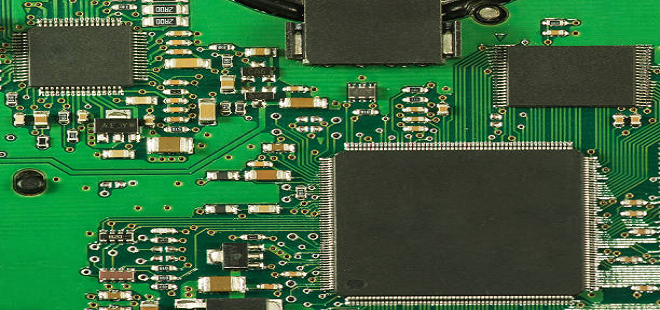
In the realm of modern technology, Integrated Circuits (IC) stand as the unsung heroes, silently powering the devices that have become an integral part of our daily lives. While we often marvel at the sleek exteriors of our gadgets, it’s the intricate architecture of IC chips that truly deserves our attention. These tiny wonders pack an enormous amount of functionality into a minuscule space, enabling the sophisticated operations that we often take for granted. In this exploration, we will delve into the fascinating world beneath the surface, uncovering the layers of complexity that define the architecture of IC chips.
The Foundation: What is an Integrated Circuit?
At its core, an Integrated Circuit is a miniature electronic circuit sold by many electronic parts supplier that incorporates multiple components like transistors, resistors, and capacitors on a single semiconductor wafer. The journey of ICs started in the mid-20th century, revolutionizing the electronics industry by replacing the cumbersome and less efficient discrete circuits.
Evolution of ICs
- First Generation (SSI and MSI): The initial foray into ICs witnessed the creation of Small-Scale Integration (SSI) and Medium-Scale Integration (MSI) chips, capable of housing tens to hundreds of transistors.
- Second Generation (LSI and VLSI): With advancements, Large-Scale Integration (LSI) and Very Large-Scale Integration (VLSI) emerged, accommodating thousands to millions of transistors, paving the way for more complex and powerful electronic devices.
- Current Trends (ULSI and Beyond): Today’s ICs fall into the realm of Ultra-Large Scale Integration (ULSI) and beyond, with billions of transistors on a single chip, enabling the creation of cutting-edge processors and memory modules.
Layers of Complexity: Anatomy of an IC Chip
The architecture of an IC chip is a marvel of engineering, consisting of multiple layers that work in harmony to execute intricate functions. Let’s peel back the layers and understand the anatomy of these technological marvels.
1. Substrate Layer
- The foundation of an IC chip is the substrate layer, typically made of silicon, which provides a stable platform for building the circuit.
- The substrate is meticulously prepared, ensuring purity and uniformity to facilitate optimal performance.
2. Transistors: The Building Blocks
- Transistors serve as the fundamental building blocks of ICs, acting as switches that control the flow of electric current.
- MOSFETs (Metal-Oxide-Semiconductor Field-Effect Transistors) are the most common type of transistors found in modern ICs, offering high efficiency and scalability.
3. Interconnect Layers
- To connect the myriad transistors, interconnect layers are introduced, typically made of metal (like aluminum or copper).
- These layers form a complex network of pathways, allowing electrical signals to traverse the chip efficiently.
4. Dielectric Layers
- Dielectric layers are sandwiched between interconnect layers to insulate them and prevent interference, enhancing the reliability and performance of the IC.
5. Packaging and Bonding Wires
- Once the chip is fabricated, it undergoes packaging to protect it from environmental factors and facilitate easy integration into electronic devices.
- Bonding wires connect the IC to the external pins, enabling communication with other components on a circuit board.
The Manufacturing Process: Bringing ICs to Life
The creation of ICs by integrated circuit distributor involves a meticulous manufacturing process known as semiconductor fabrication. Understanding this process gives us insight into the precision required to produce these intricate chips.
1. Photolithography
- Photolithography is a crucial step where a light-sensitive material is used to transfer the intricate circuit patterns onto the substrate.
- Ultraviolet light is directed through a mask, creating a pattern on the substrate.
2. Etching
- Etching involves removing material from the substrate according to the pattern created in the previous step.
- Chemical or physical methods are employed to selectively remove material, leaving behind the desired circuit pattern.
3. Deposition
- In the deposition phase, layers of materials, including conductors and insulators, are deposited onto the substrate to build the circuit.
4. Doping
- Doping introduces impurities into the semiconductor material to modify its electrical properties, creating regions with specific conductivity.
5. Testing and Packaging
- Rigorous testing is conducted at various stages to ensure the functionality and reliability of the IC.
- Once verified, the ICs are packaged, marking the final stage before integration into electronic devices.
Challenges and Future Prospects
While ICs have come a long way, the industry faces ongoing challenges. As transistors shrink to nanoscale dimensions, issues such as heat dissipation and quantum effects become more prominent. Researchers are exploring innovative materials and designs to overcome these challenges and usher in the era of quantum computing.
Conclusion
In the grand tapestry of technology, Integrated Circuit chips weave a tale of innovation, precision, and relentless progress. Beneath the surface of our sleek devices lies a world of microscopic wonders, where transistors dance in orchestrated harmony, and layers of complexity give birth to the seamless experiences we enjoy every day. As we navigate the future, the architecture of IC chips will continue to evolve, pushing the boundaries of what’s possible and shaping the next chapter in the story of human ingenuity.
